PPG Heart Rate Detection Circuit & PCB
Designed a BJT monostable multivibrator, edge differentiator, and LED driver circuit targeting 180 BPM detection, validated in LTSpice, and manufactured through JLCPCB.
Date
2026-03-01
Role
Analog Circuit & PCB Designer
Stack
Demo
Overview
A full analog signal chain for photoplethysmography (PPG) heart rate detection. Goes from raw optical signal to a clean digital pulse suitable for timing. The target was reliable detection up to 180 BPM, designed entirely with discrete BJTs and passive components.
Signal Conditioning
Raw PPG signals from a photodiode are low-amplitude and high-noise. The front-end uses a transimpedance amplifier stage followed by a BJT-based amplification and filtering chain to improve signal-to-noise ratio before the timing detection stage. The filter roll-off was set to suppress motion artifact and 50/60 Hz mains interference while preserving the fundamental pulse frequency band.
Monostable Multivibrator & Edge Differentiator
The conditioned signal feeds a BJT monostable multivibrator that produces a clean fixed-width output pulse on each detected heartbeat. An edge differentiator upstream ensures only the rising edge of the conditioned waveform triggers the monostable, preventing double-triggering from signal ringing.
The LED driver stage converts the monostable output to a visible indicator pulse, giving a real-time visual confirmation of each detected beat during bench testing.
PCB Layout & Manufacturing
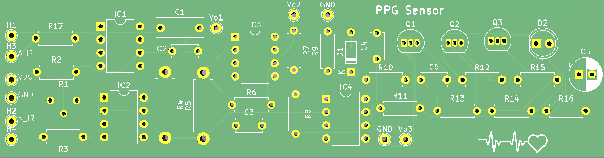
Laid out the full schematic-to-PCB flow in KiCad, with careful attention to:
- Short trace routing on the high-impedance photodiode input to minimize capacitive pickup
- Ground plane continuity under the analog signal path
- Test points on every major node for oscilloscope probing
Boards were manufactured through JLCPCB and validated against simulation waveforms on the oscilloscope.
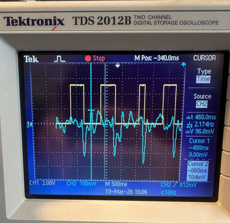
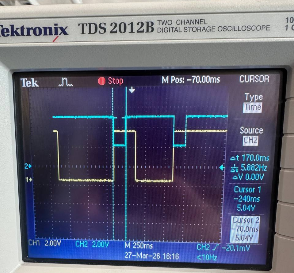
Simulation & Validation
All timing-critical stages were validated in LTSpice before layout. Simulated timing accuracy was within ±10 ms of target at the design corner. The simulation models also helped identify the correct biasing resistors for the BJT stages across temperature.
Bench measurements confirmed the design. The oscilloscope captures below show the raw PPG signal and the clean monostable output pulses on the manufactured board.